
_Numerous memory types for computing devices have emerged in recent years, aiming to overcome the limitations imposed by traditional random access memory (RAM). Magnetoresistive RAM (MRAM) is one such memory type which offers several advantages over conventional RAM, including its non-volatility, high speed, increased storage capacity and enhanced endurance. Although remarkable improvements have been made to *MRAM devices, reducing energy consumption during data writing remains a critical challenge.
A study recently published in Advanced Science by researchers from Osaka University proposes a new technology for MRAM devices with lower-energy data writing. The proposed technology enables an electric-field-based writing scheme with reduced energy consumption compared to the present current-based approach, potentially providing an alternative to traditional RAM.
Conventional dynamic RAM (DRAM) devices have basic storage units consisting of transistors and capacitors. However, the stored data is volatile, meaning that energy input is required to retain the data. In contrast, MRAM uses magnetic states, such as the orientation of magnetization, to write and store data, enabling non-volatile data storage.
“As MRAM devices rely on a non-volatile magnetization state rather than a volatile charge state in capacitors, they are a promising alternative to DRAM in terms of their low power consumption in the standby state,” explained Takamasa Usami, lead author of the study.
The present MRAM devices generally require an electric current to switch the magnetization vectors of magnetic tunnel junctions, analogous to switching capacitor’s charge states in a DRAM device. However, a large electric current is needed to switch the magnetization vectors during the writing process. This results in inevitable Joule heating, leading to energy consumption.
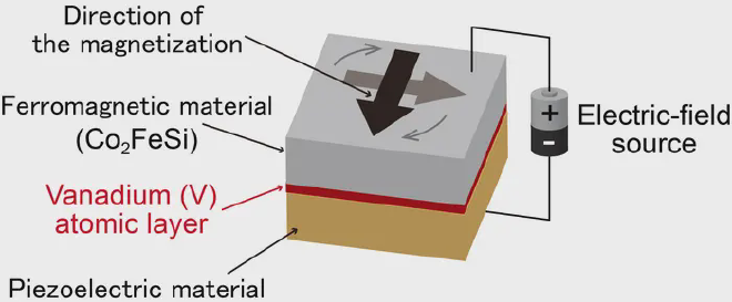
To address the problem, the researchers have developed a new component for electric field controlling of MRAM devices. The key technology is a multiferroic heterostructure with magnetization vectors that can be switched by an electric field (featured image). The response of the heterostructure to an electric field is basically characterized in terms of the converse magnetoelectric (CME) coupling coefficient; larger values indicate a stronger magnetization response.
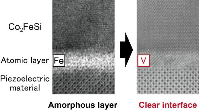
The researchers previously reported a multiferroic heterostructure with a large CME coupling coefficient over 10-5 s/m. However, structural fluctuations in parts of the ferromagnetic layer (Co2FeSi) made it challenging to achieve the desired magnetic anisotropy, hindering reliable electric-field operation. To improve the stability of this configuration, the researchers developed a new technology for an insertion of an ultra-thin vanadium layer between the ferromagnetic and piezoelectric layers. As shown in Fig. 2, a clear interface was achieved by inserting the vanadium layer, leading to the reliable control of the magnetic anisotropy in the Co2FeSi layer. Also, the CME effect reached a value larger than that achieved with similar devices that did not include a vanadium layer.
The researchers also demonstrated that two different magnetic state can be reliably realized at zero electric field by changing the sweeping operation of the electric field. This means a non-volatile binary state can be intentionally achieved at zero electric field.
This research in spintronic devices could eventually be implemented on practical MRAM devices, enabling manufacturers to develop ME-MRAM, which is a low-power writing technology for a wide range of applications requiring persistent and safe memory.
- The article “Artificial control of giant converse magnetoelectric effect in spintronic multiferroic heterostructure,” was published in Advanced Science. Authors: Takamasa Usami, Yuya Sanada, Shumpei Fujii, Shinya Yamada, Yu Shiratsuchi, Ryoichi Nakatani, Kohei Hamaya